Published in 1998
Introduction
As the critical dimension for VLSI circuits is scaled deeper into the submicron range and wafer size grows, requirements for wafer to wafer temperature repeatability during processing become more demanding. Virtually every process step in silicon wafer fabrication depends on the measurement and control of wafer temperature.
Processes such as PVD, HDP-CVD and RTP can be improved if wafer temperature is accurately measured and controlled during processing. In RTP there’s a special importance to temperature monitoring because of the high temperatures and the importance of tightly controlling the thermal budget.
As wafer sizes increase, the cost of each wafer grows and the value of high quality in-process temperature monitoring becomes critical. Inadequate control of wafer temperature during processing reduces fabrication yields and directly translates to lost revenues amounting to tens of thousands of dollars.
Temperature monitoring / measurement techniques
The most common techniques used in wafer fabs and foundries for in-situ temperature sensing in the semiconductor processing environment are:
- Thermocouples
- Conventional Pyrometry
- Advanced Pyrometry
Other temperature measurement methods do exist, but their use is mostly limited to R&D. As far as wafer production is concerned, the only method which offers a satisfactory temperature monitoring solution is Advanced Pyrometry.
Thermocouples
Thermocouples are easy to use, however their reliability and accuracy are highly questionable. They are only accurate when the wafer is in thermal equilibrium with it’s surroundings and the thermocouple is embedded in that environment. When this condition is not met, the thermocouple reading might be very far from the true wafer temperature. For example in PVD, the thermocouple embedded in the heated chuck, gives a temperature reading which resembles that of the wafer in a fairly reasonable manner - but only before the process actually begins. When the plasma deposition process actually starts, the wafer temperature changes significantly, but the thermocouple reading is hardly affected!
Conventional Pyrometry
Another popular technique is Optical Pyrometry. A pyrometer deduces the wafer temperature from the intensity of the radiation emitted by the wafer. The relation between the intensity of the radiation and the wafer temperature is given by Plank’s law which shows that the radiation emitted by any object is a function of it’s temperature, emissivity and the wavelength of measurement.
The common way of using a pyrometer, is collecting the radiation from the wafer using a quartz or sapphire rod.
This type of interface has been used with PVD, HDPCVD, RTP, Etch and RTCVD equipment offered by several major reactor vendors. While this technique is superior to the use of thermocouples, there are some problems of inaccuracy in the actual processing environment, which cannot be ignored [1].
Advanced Pyrometry
Advanced Pyrometry takes into account the limitations of Conventional Pyrometry and incorporates methods for overcoming them.
Wafer emissivity
Emissivity is a characteristic of the wafer, it’s value ranging from 0 to 1. The higher the wafer’s emissivity is, the more energy it emits. For a wafer at a given temperature, the wafer emission is a linear function of the emissivity.
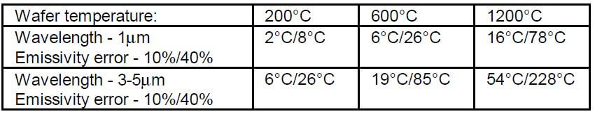
The fact that wafer emission depends so strongly on emissivity means that even the best Pyrometer will result in large temperature errors if wafer emissivity is not accurately known. Dependence of wafer emissivity on layer thickness is shown in Figure 1 for PolySilicon on oxide (simulation results).
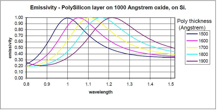
Figure 1 - Emissivity of a Si wafer with a 1000Å Oxide layer and a Polysilicon layer of varying thickness. The figure shows that at any given pyrometer wavelength, emissivity can widely vary due to slight changes in layer thickness.
Several examples for the translation of emissivity errors to temperature errors are given in the following table:
1. Instead of measuring wafer temperature, measure the temperature of an object which is thermally connected to the wafer, with known emissivity. This solution has limited accuracy (to the extent that the two bodies can be thermally coupled) and is not very production oriented.
2. Measure emissivity of a typical wafer off-line and use it as input to the Pyrometer. The accuracy of this method is limited by the repeatability between the backsurface emissivity of the different wafers represented by this one wafer. Another problem is that some layer configurations cause serious temperature dependent emissivity changes.
3. Measure emissivity of all wafers in a separate chamber, before they enter the process chamber [2]. This solves one of the above mentioned problems and works quite well for most wafers. The only problem left unsolved is the emissivity dependence on temperature. Another issue is the need to have some space allocated on the cluster tool for the purpose of emissivity measurement.
4. The best solution from all aspects would be real time in-situ emissivity measurement at the same point of temperature measurement. This solution offers simple, compact, Pyrometer interface with accurate emissivity estimation through the whole temperature range. The signal used for the emissivity estimation is measured in the same detection system as the signal emitted from the wafer. The signals are then separated in the system
electronics.
Background
Background is any radiation source, other than the wafer, which might cause stray radiation to arrive at the detection system (the Pyrometer). This might be plasma, radiation from a heated chuck or from lamps employed as a heat source. As shown in Figure 2, background radiation might reach the rod directly, or be reflected from the wafer into the light collection system, or pass through the wafer.
These sources of background radiation are handled in different ways:
Stray radiation – In RTP, radiation from the lamps may reach the pyrometer optics (Figure 2 - (b)). The intensity may even be such as to cause saturation of the pyrometer. Even if it does not do so, the stray radiation causes an error in temperature measurement. The most common solution is to block the radiation.
Radiation from heater – when the wafer is placed on a heated chuck (as for example in most PVD reactors), radiation from the chuck enters the light pipe, either directly, or via reflections from the wafer (Figure 2 - (a)). This type of radiation can be compensated for, as the radiation is related to the known chuck temperature. Lack of compensation may cause large errors, especially in cases where either the wafer temperature is significantly lower than that of the heater, or wafer emissivity is low.
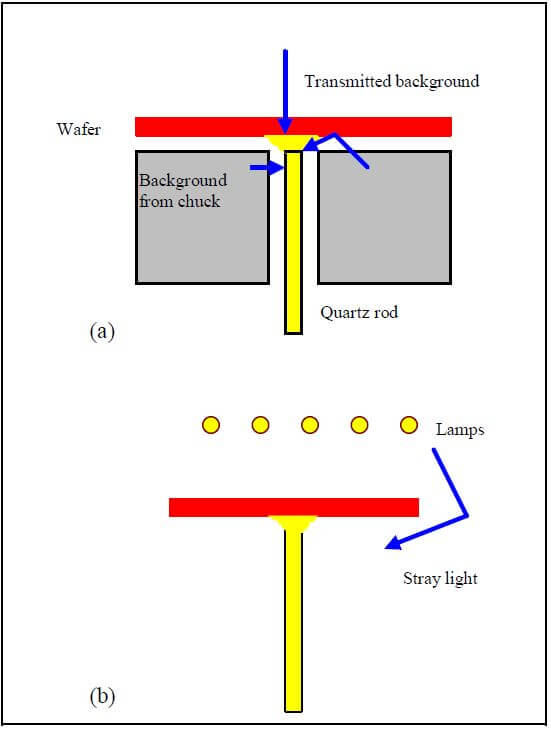
Figure 2 - (a) In-chamber radiation source interference in a heated chuck type of system. (b) In-chamber radiation sources in a system where the wafer is heated by lamps.
Radiation through the wafer – A Silicon wafer in room temperature is opaque up to about .95 microns. Above
this wavelength it’s transmission is relatively high, unless opaque layers are grown on the wafer. This means that any radiation source above the wafer would be seen by the pyrometer. As the wafer is heated, the band edge of the substrate shifts [3], and the wafer becomes opaque up to higher wavelengths. The graph shown below (Figure 3) was measured on an HDP CVD reactor from one of the main vendors, for a bare Silicon wafer. The graph shows the initial spike resulting from the onset of plasma, the large signal resulting from the plasma as seen through the wafer. As the wafer becomes gradually opaque, the signal drops. At a certain point the wafer is completely opaque and true temperature measurement begins.
Signal to Noise Ratio (SNR)
Pyrometer SNR performance depends on two main issues:
- Electronics and optics design quality.
- Wavelength - Both the amount of signal emitted by the wafer, and the rate of change of signal per temperature ( radiance contrast ), depend strongly on the Pyrometer wavelength. Wavelength around 1mm results in signal levels high enough for the semiconductor processing applications, it also has relatively high radiance contrast (i.e. large signal difference for a given temperature change) and is therefore more immune to errors resulting from noise, background and emissivity estimation inaccuracy.
The better the Pyrometer’s SNR, the lower the minimum temperature that can be achieved and the better accuracy and repeatability of the temperature readings.
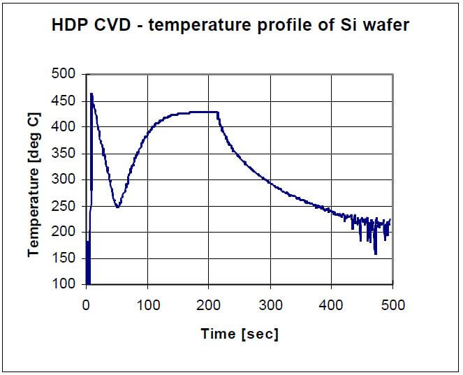
Figure 3 - HDP CVD - Si wafer temperature measurement. Onset of plasma results in large reading through transparent wafer. At 250°C the wafer becomes opaque at the measurement wavelength and true temperature measurement begins. Signal starts to drop when plasma is turned off and wafer cools down. True temperature measurement continues as low as 230 °C.
Pyrometer specifications
Standard Pyrometers usually have quite impressive specifications as far as accuracy and repeatability are concerned. These specifications are indeed valid, but only when measuring a known calibration target under laboratory conditions. As seen in the previous sections, once under real production conditions, in various applications, performance will be degraded as a result of background and emissivity errors. Under these conditions, the intrinsic pyrometer specifications becomes virtually meaningless. The relevant specifications should relate to in-situ conditions and may be application dependent.
Applicability and Benefits of Advanced Pyrometry In the previous sections we showed that Advanced Pyrometry is the only solution for high quality, in-situ temperature monitoring. To summarize, Advanced Pyrometry must incorporate:
1. Low wavelength measurement (around 1mm), to ensure good accuracy and repeatability, as well as low sensitivity to emissivity estimation errors.
2. Good SNR, to allow low minimum temperature plus high accuracy and repeatability.
3. Background compensation - application dependent background compensation, by hardware and
software means.
4. Real time, in-situ same point emissivity measurement and compensation.
The combination of all these features contributes to higher yields in many of the semiconductor’s industry key production processes, such as PVD, HDP-CVD, and RTP. When first introduced, Advanced Pyrometry was perceived to be a “Nice-to-Have” feature, but in today’s world of larger size wafers and submicron processing, it has become “Must Have” equipment that cannot be ignored.
References
[ 1 ] Emissivity compensated, radiance contrast tracking pyrometry for semiconductor processing. M.E. Adel, S.Mangan, Y. Ish-Shalom. SPIE Vol. 2091, September 93.
[ 2 ] True wafer temperature during metallization in Physical vapor deposition cluster tools. M.E. Adel, S.Mangan, H. Grunes, V. Parkhe. SPIE Vol. 2336, October 94.
[ 3 ] Substrate temperature measurement by absorption-edge spectroscopy during molecular beam epitaxy of narrow-band gap semiconductor films. T.J. de Lyon, J.A. Roth, D.H. Chow. J. Vac. Sci. Technol. B 15(2), 1997.