Non-contact Temperature Sensors
CI Semi's family of noncontact temperature monitors (the NTM line), offers high end pyrometry products for the measurement of wafer temperatures during process.
CI Semi’s flag ship of the line, the NTM Delta, incorporates real-time, same point emissivity measurement and compensation making it the ideal solution for in situ monitoring for processes such as RTP, CVD and PVD. The NTM family is sold to leading tool manufacturers.
CI's NTM product line offers a variety of pyrometers, with and without emissivity measurement, from visible to short (NIR) and long IR wavelength. These pyrometers can be used for in situ true temperature measurement and/or reflectivity (single wavelength) during production.
Wafer Temperature Monitoring
CI Semi’s specialty is in-situ, noncontact wafer temperature monitoring. In many cases, obtaining the best results requires close collaboration with the equipment manufacturer, so as to optimally address such issues as interfering radiation, and geometrical constraints. CI Semi works closely with customers to customize and integrate wafer temperature monitors on many different tools. Some of the major challenges are discussed below.
Wafer Transparency & Minimum Measurable Temperature
There are plenty of pyrometers in the market that are able to measure down to room temperature. These typically operate at long wave IR bands (MWIR and LWIR), which translates to more energy (see Plank’s curve – figure 1a). When measuring a Silicon substrate we need to take into consideration the transmission curve of the wafer. A cold wafer is transparent at wavelengths over ~1 micron and, as such, cannot be measured in the LWIR.
In the NIR the wafer emission is very low, so an extremely sensitive pyrometer is required.
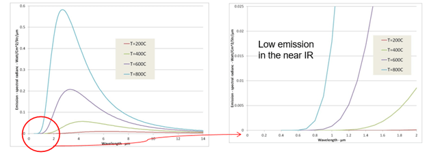
Figure 1 – Blackbody emission, according to plank’s law. (a) NIR through LWIR (b) Close up on NIR – very low emission, requiring high sensitivity to monitor.
CI Semi offers NIR pyrometers that can measure as low as 180C.
Background Radiation
The main approach to wafer temperature measurement is based on measuring the self emission of the wafer, which according to Plank’s law is a function of the wafer temperature and emissivity. When measuring wafer emission in a semiconductor reactor, one may inadvertently measure radiation from other sources as well – a lamp or LED heaters, resistive heater, plasma.
_20210321164245.225.png)
CI Semi’s approach involves close interaction with the equipment vendor, studying the radiation characteristics and using hardware and software approaches to reduce, or eliminate, the impact of those sources.
Our approaches include:
- Subtraction of background through software - estimating or measuring background radiation and subtracting that in software, potentially using direct input (analog or digital) from the tool.
- Optical filtering – depending on the radiation source (lamps, plasma, resistive heater), different optical filtering can optimize the measurement.
- Synchronization – the system electronics and software can allow synchronization of the measurement with the cycle time of the heater, allowing monitoring at a time when the heater is off, even for very high frequency heaters.
Emissivity Measurement and Compensation
When monitoring temperature based on the self-emission of the wafer (pyrometry), one needs to take into account, that depending on film structure on the face of the wafer measured, the emissivity of the wafer may vary. The measured emission is a function of both wafer temperature and wafer emissivity. In order to accurately extract temperature, emissivity needs to be properly estimated. CI Semi’s NTM Delta allows for real time, same point, active emissivity measurement and compensation. The measurement is achieved via reflectivity measurement.
If true wafer emissivity is not known, and one assumes that all wafers have the emissivity of a bare wafer (.68 at ~1 micron), the resulting errors can be significant:
_20210321164827.991.jpg)
Multi-point Measurement
With 12” wafers and multi-zone heaters, it can be of interest to measure temperature in multiple points. CI Semi offers dual point models, and the ability to synchronize multiple units with each other, allowing for example single point emissivity measurement, and sharing the emissivity measurement with the other probes, measuring emission only for those, for a more cost effective solution.